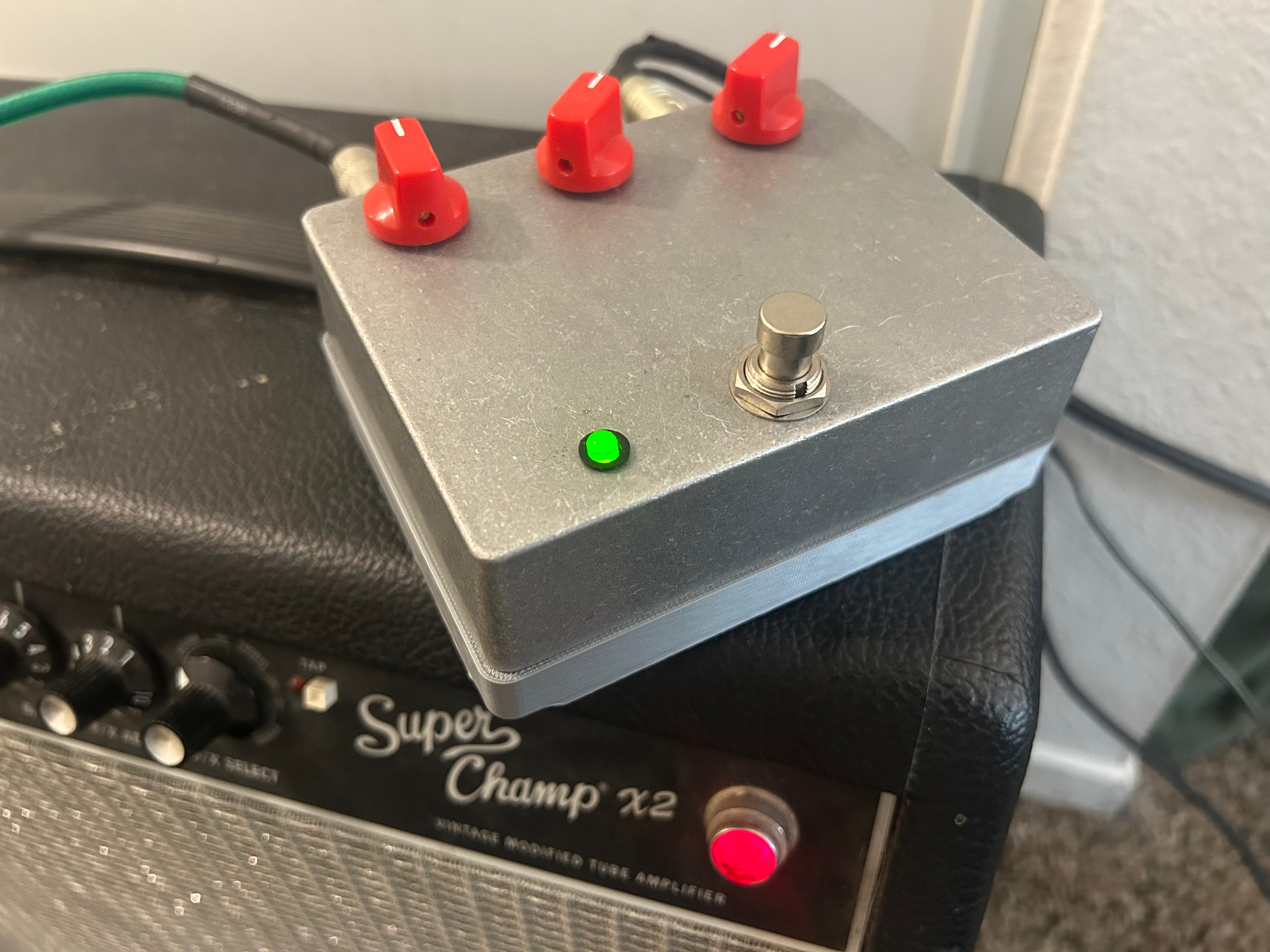


I recently saw my friend Rex’s band play a show, and he mentioned that he needed a reverb pedal. I decided to find a schematic and build him one to learn about op-amp configuration, biasing, filtering, frequency response, and oscillation. I also modeled the pedal’s circuit in LTSpice, measured values with an oscilloscope, and modded the original schematic to make it more interesting.
Prototype Build

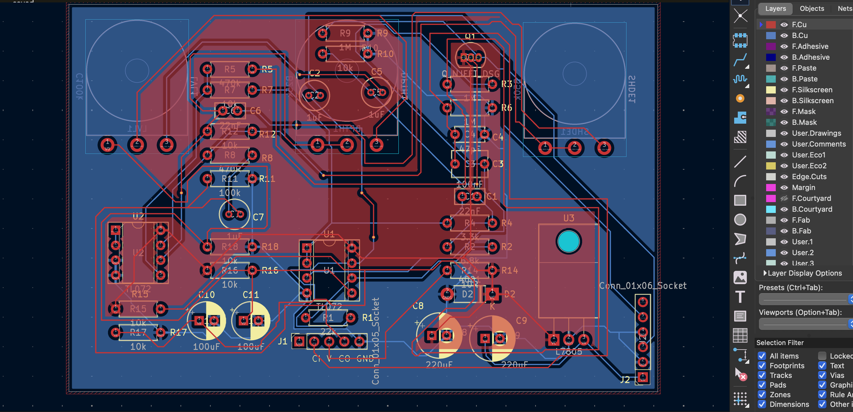
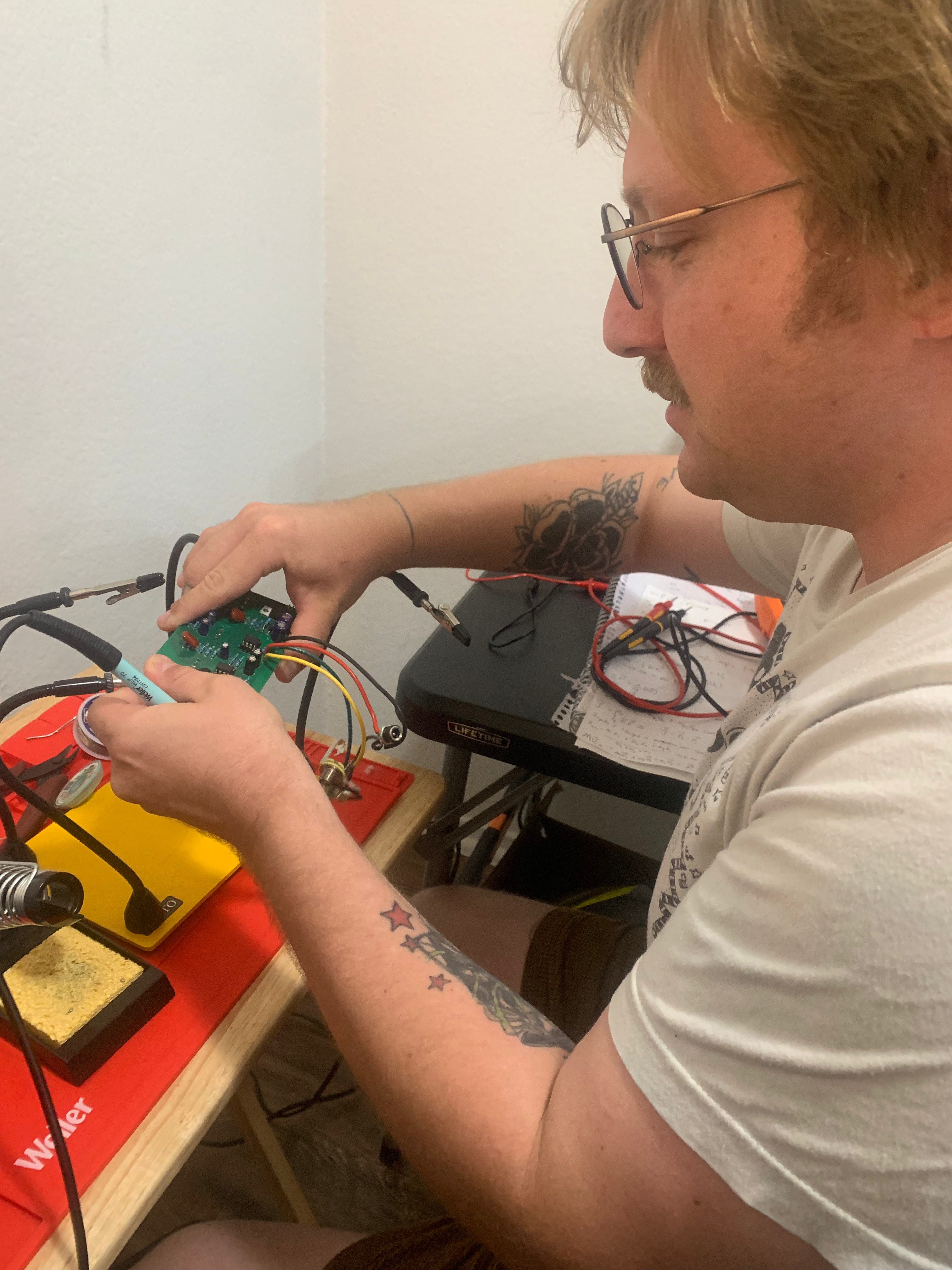
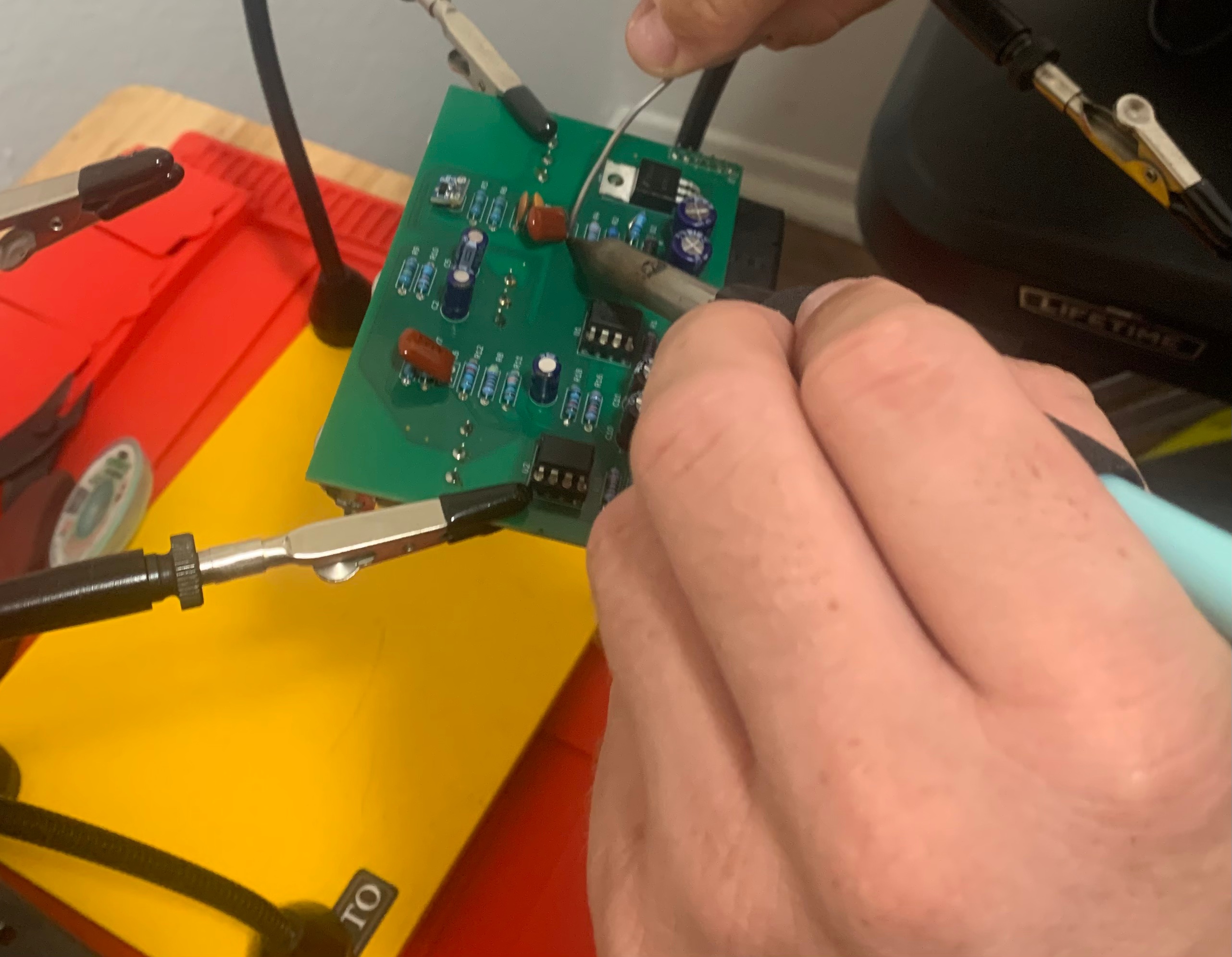
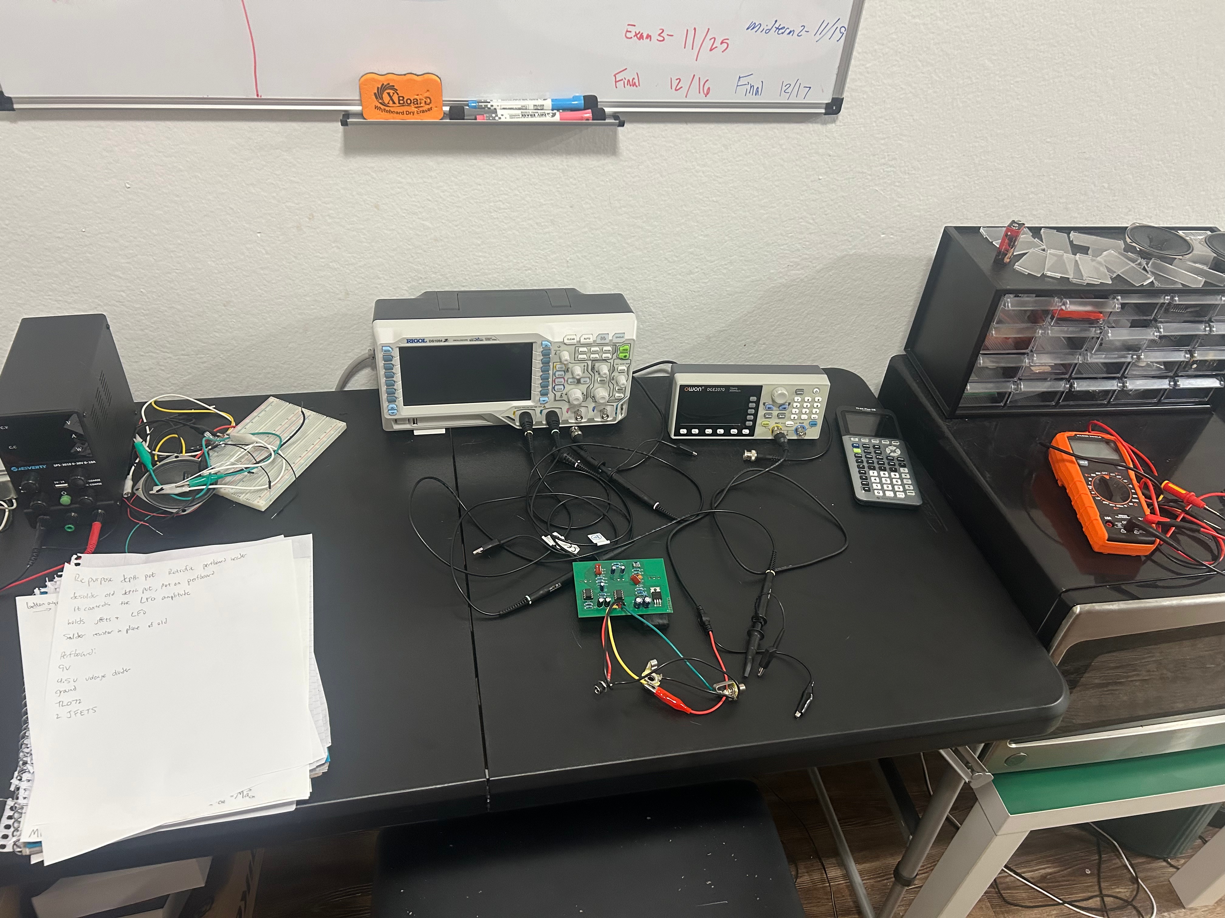
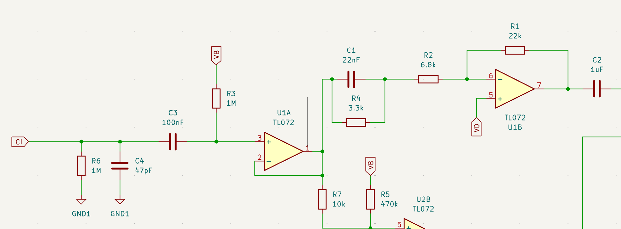
Once I sourced a suitable schematic for a reverb pedal online, I opened KiCad and re-made each stage of the circuit until I had the full pedal in schematic capture, designed the PCB, and got it printed and shipped. I also made a bill of materials and ordered components from DigiKey and Jameco. Using my soldering station, I populated the board and wired jacks to it for prototype testing.

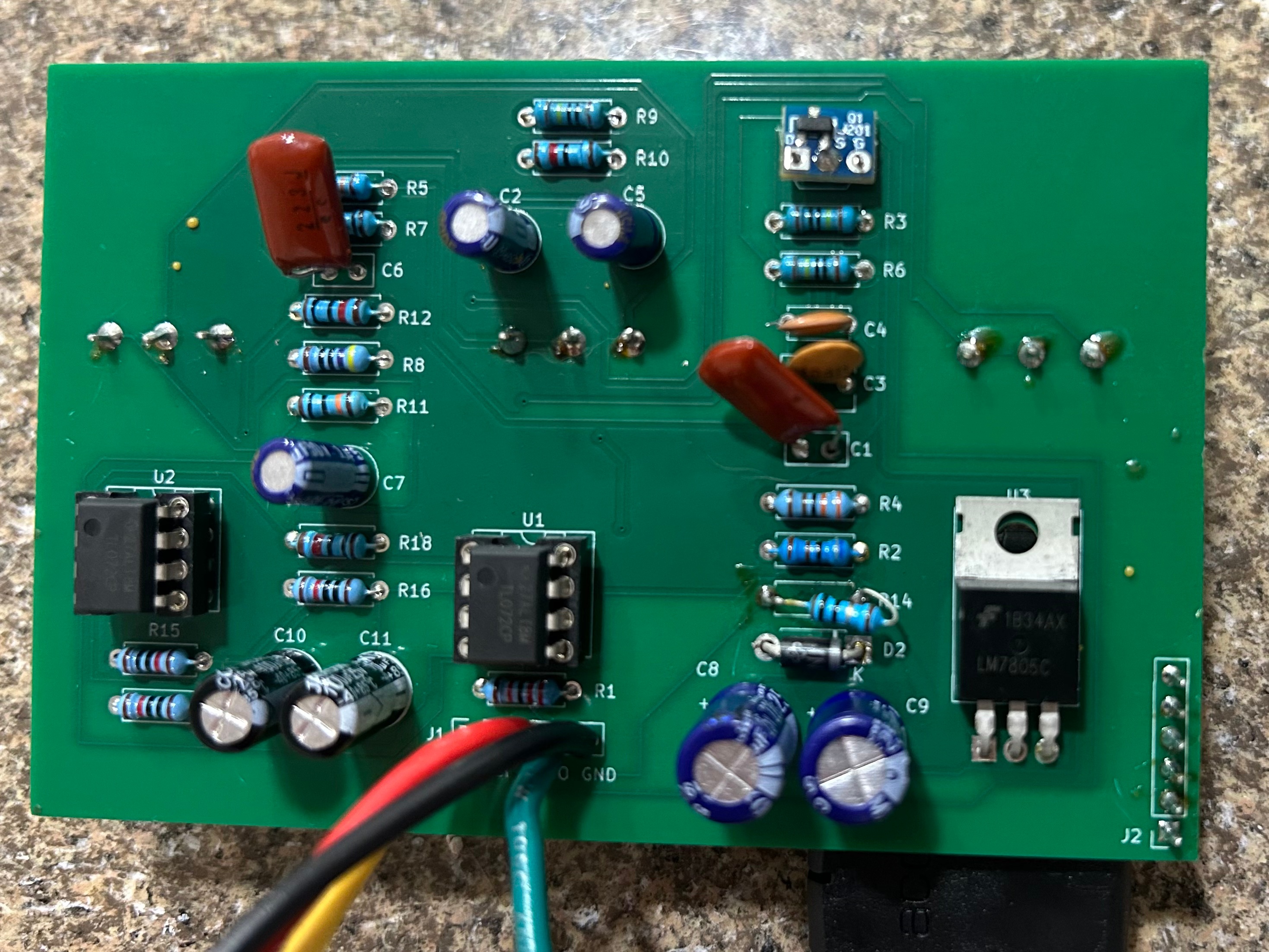

Plugging it in for the first time, I didn’t get any sound. After I unplugged it, I noticed a discolored resistor. It was R14, the resistor right next to the power supply. I figured this resistor was possibly shorted, and therefore slightly burned.
I cut the burned resistor’s leads and replaced it with a new one, then looked at the schematic to start troubleshooting.
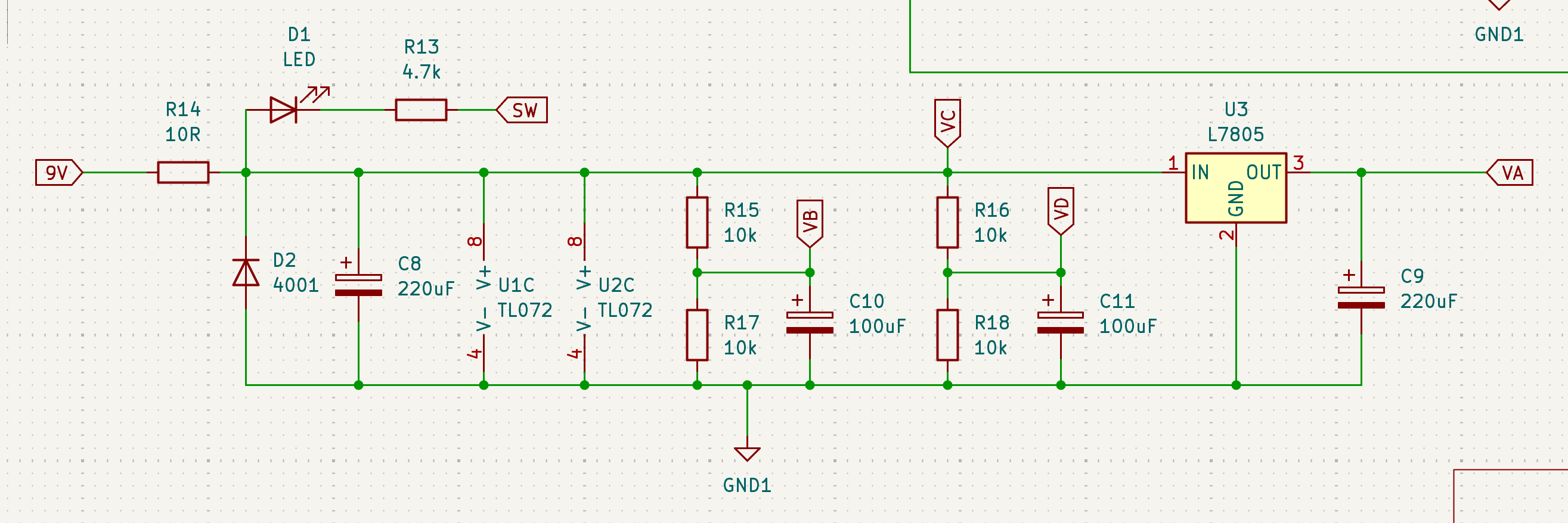
This section takes 9 volts and distributes it to the indicator LED, two TL072 op-amps, and a JFET transistor.
Voltage dividers make a bias voltage of 4.5V to act as a virtual ground for the guitar signal to swing around.
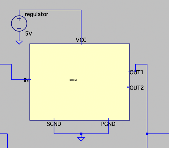
A 7805 linear voltage regulator brings supply voltage down to 5V to power the reverb IC properly, according to its datasheet.
Bypass/decoupling capacitors are placed right before each branch of power output, shunting high frequency noise and smoothing current spikes.
Lastly, there’s a diode for reverse-polarity circuit protection. If voltage is applied backward, it will short the entire circuit except for one 10 Ohm resistor, protecting the pedal but decimating the sacrificial resistor. This was the burned resistor from earlier! The power supply I had was the opposite polarity of what I should’ve used.
Luckily, the board was just fine, so I bought the right power supply, hooked up my guitar, and it actually worked!
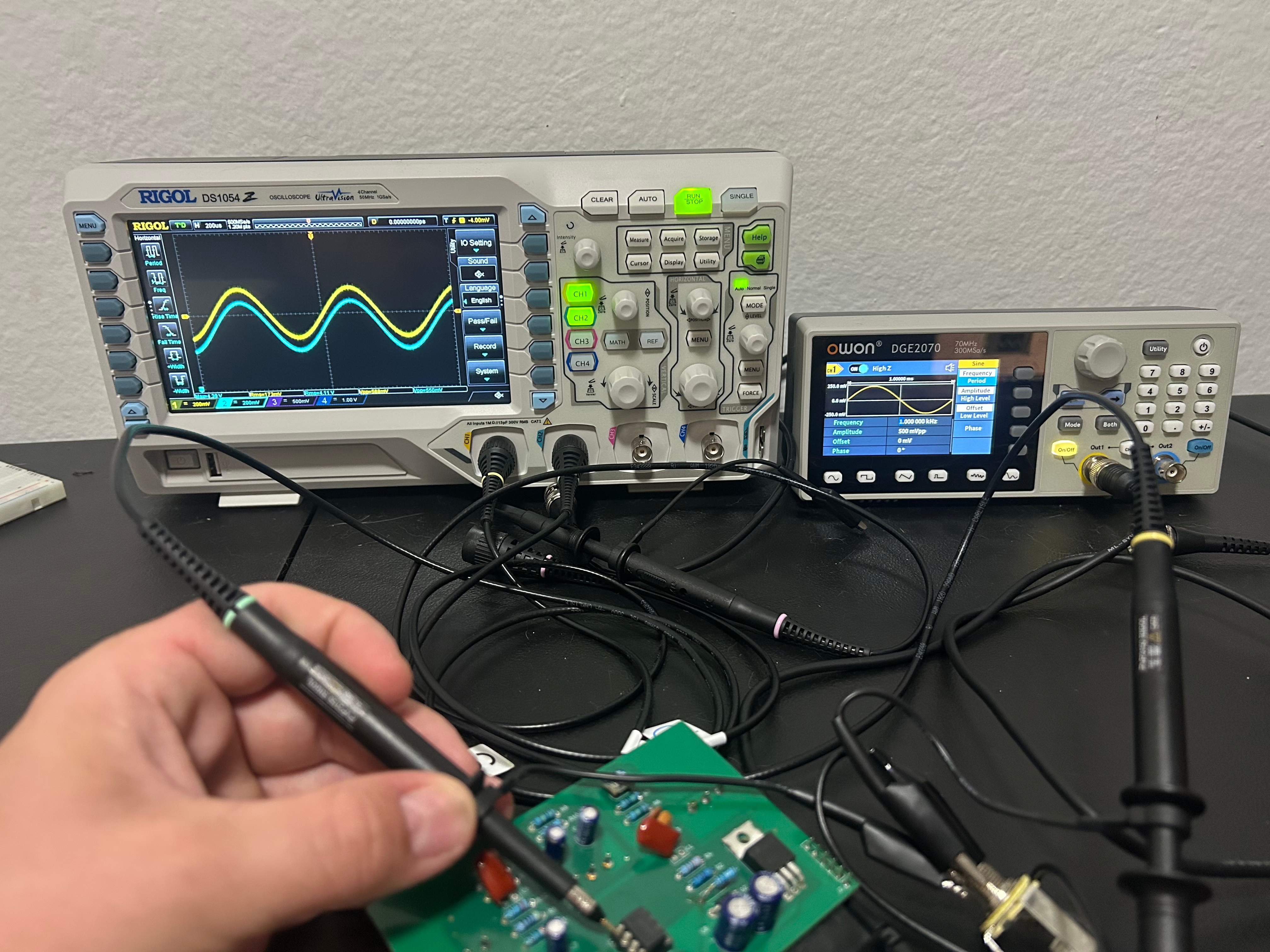
Now that I’d built a working prototype, I decided to analyze the signal flow by modeling it in LTSpice and comparing the results with oscilloscope measurements.
Signal Analysis
Preamp
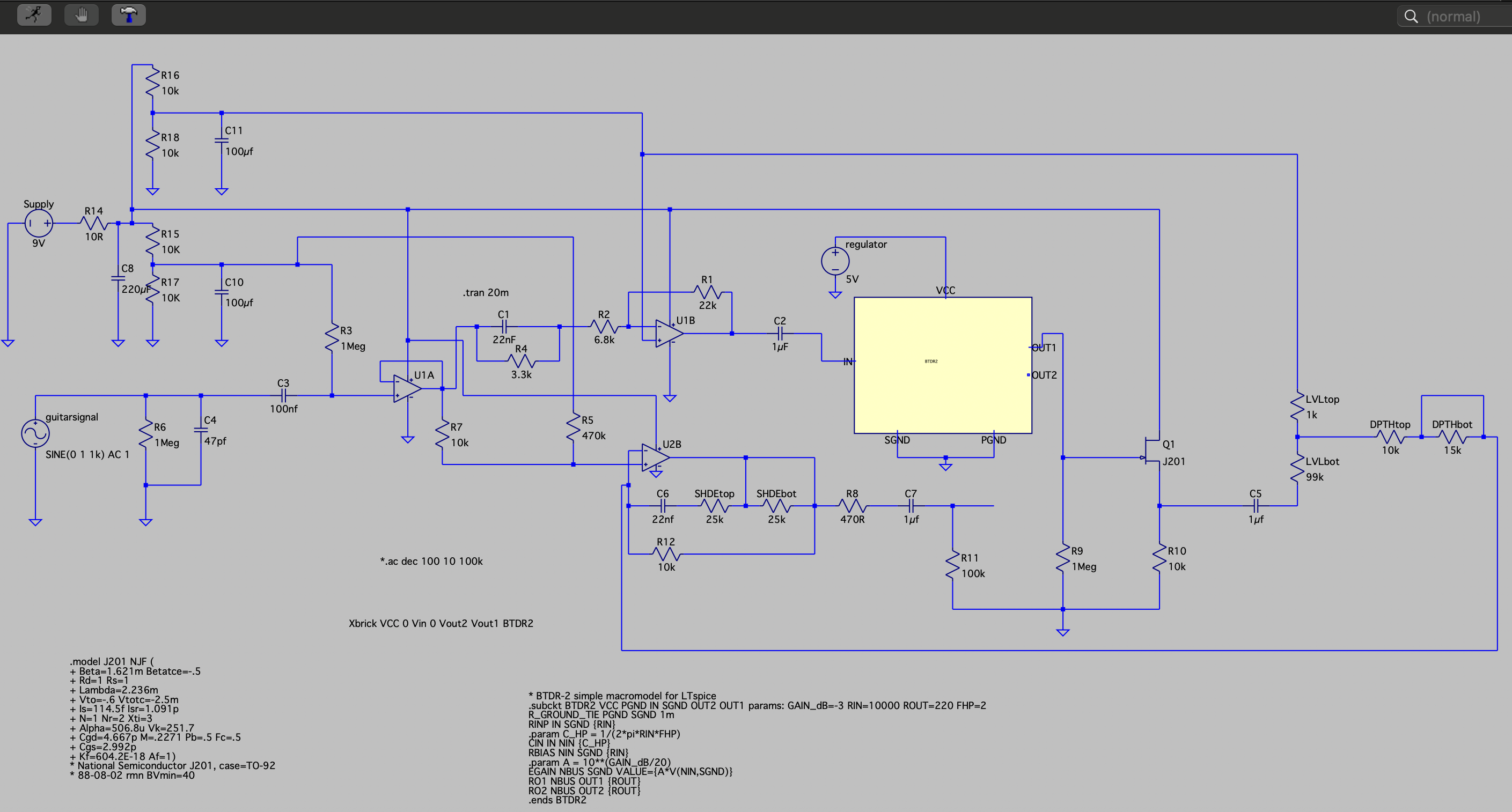
The guitar signal comes from CI (the input jack of the pedal) and is given ground reference through R6. This 1M resistor is large, so it doesn’t load the pickups. C3 couples the signal, blocking any DC offset.
The signal is then fed into U1A, which is a non-inverting follower, isolating the guitar from the rest of the pedal with high input impedance.
VB is the 4.5V bias, which ensures there is no negative voltage present in the signal for the op-amp, a technique known as single supply biasing. This is necessary because the op-amp’s negative supply voltage pin is at ground.
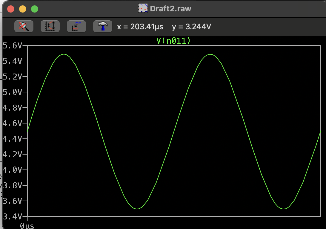
Transient simulation in LTSpice showed what I expected at U1A: a sine centered at 4.5V.
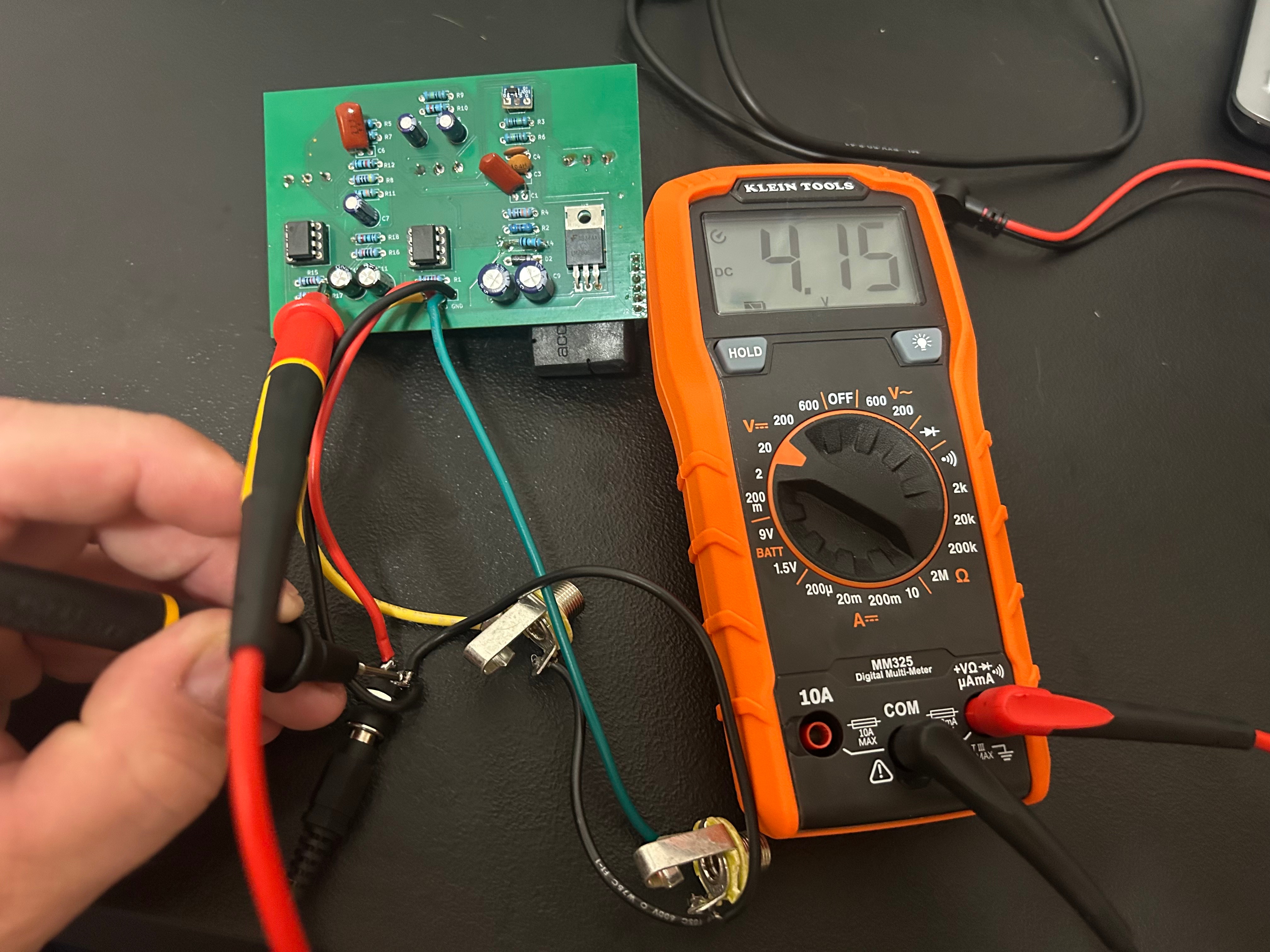
In reality, the bias voltage at the divider measured 4.15V. The wall power supply voltage was at 8.99V, so something in the circuit was causing that divided voltage to sag half a volt. Perhaps the op-amp’s input draws some current? Regardless, it didn’t affect operation and is expected of a real situation.

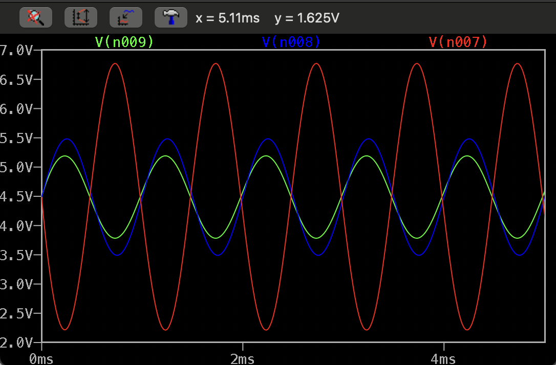
I injected a 1kHz sine and compared it to U1A’s output. Everything was as expected: the waveform was the same, but biased at 4.1V.
The signal is then filtered, amplified, and inverted before entering the digital reverb IC. U1B’s gain is frequency dependent because of C1 and R4 forming a sort of high pass filter.


An AC sweep in LTSpice showed a shelf filter. High gain above ~2kHz, less below that.
Simulation and measurement were similar. At peak to peak voltage of 500 mV, the 1kHz input signal was filtered and amplified to 1.21 Vpp. This agrees with AC sweep plot- it shows a gain of 7.2dB at 1kHz, which translates to 2.29*0.5= 1.14 V.
Digital Reverb IC

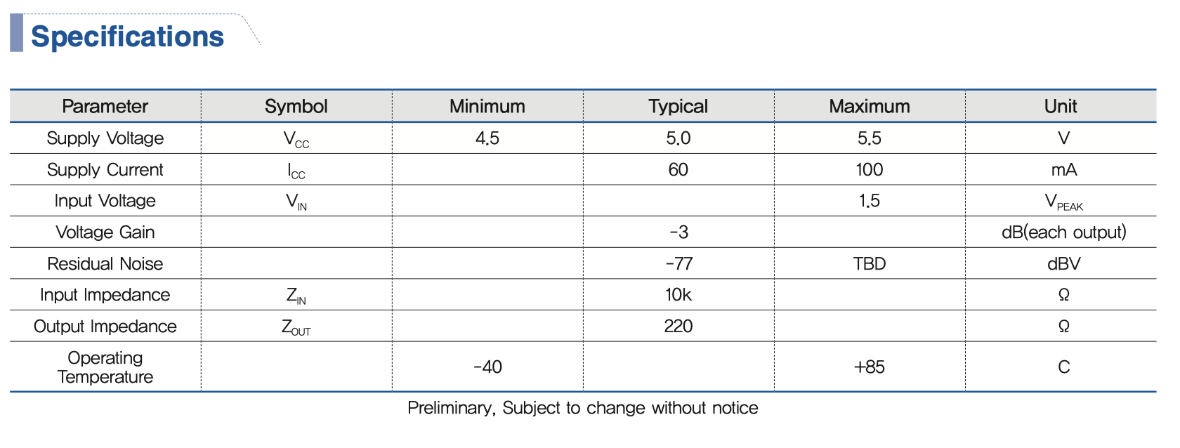
The datasheet for the reverb IC says max input voltage is 1.5V peak. Scope measurements were well within this range, so no clipping occurred. The chip’s voltage gain is -3 dB, so the output signal should be about 70% of the input. I modeled this parameter as a component in LTSpice, along with approximate input and output impedances.

The output from the chip is hard to measure on a scope, because it’s a jiggling, reverberating signal. But an average RMS measurement of the input vs output seemed reasonable: 414 mv in, about 250 mv out. Not a perfect 70% by any means, but within acceptable range.
Mixing and Output
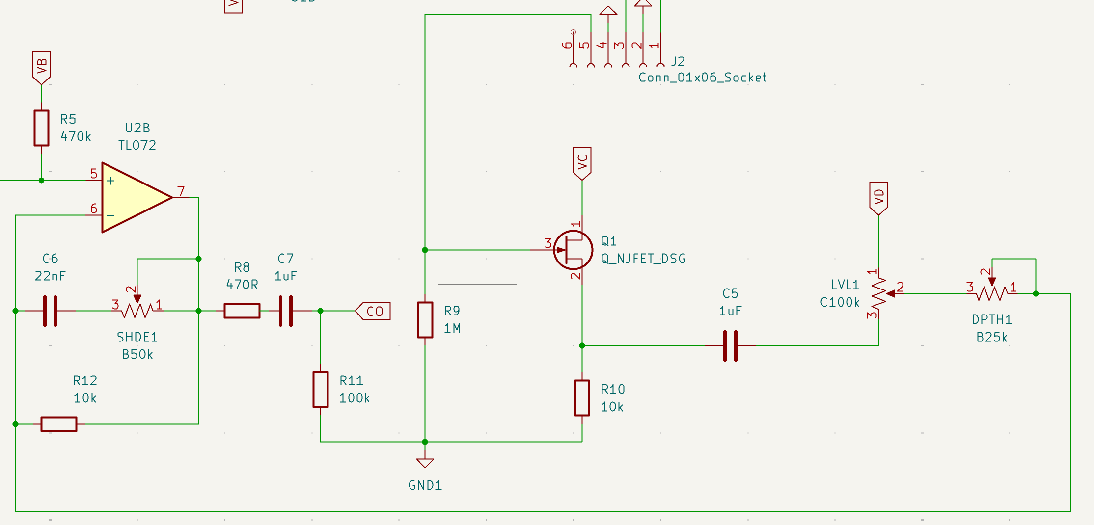
The wet reverb signal leaves the IC from pin 5 of J2 to the gate of JFET Q1. This is a source follower FET configuration; again we have a buffer that isolates one part of the circuit from the other, ensuring there’s almost no current draw on the digital IC while keeping the signal voltage about the same, although the scope measured a 2.5V bias because of the way a JFET conducts (it can’t go negative).
Potentiometer LVL1 attenuates the AC portion of the signal based on the knob’s position. This is the reverb IC’s output level.
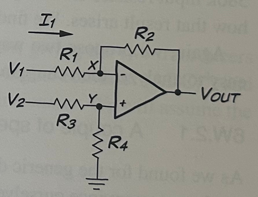
The last op-amp U2B is configured as a difference amplifier with frequency shaped feedback. Its output is the difference of the dry and wet signals, but they’re 180 degrees out of phase with each other because of the inverting amp, so they actually get added together, or mixed.
DPTH1 acts as a variable resistor that decreases the wet signal contribution to the overall output, as well as the overall output itself.


The feedback loop for U2B is two parallel paths: one with resistor R12 and the other with a variable resistor SHDE1 going through C6. This is a frequency dependent feedback loop. C6 has less impedance at high frequencies, so Zf goes down.
Less impedance in the feedback loop causes less gain, so this parallel network makes a low pass filter: it has less gain at high frequencies. The Shade knob, then, is a reverb tone control. As Shade increases its resistance, more high frequencies are output.

Each solid line is the frequency response at the output of U2B with the shade knob at a different position. As the knob turns and its resistance increases, it lets more high frequencies through to the output, resulting in brighter reverb. Keep the knob turned down, and the reverb will sound darker and muted.

Here is the frequency response of the output at different Depth knob levels. The output starts low with the knob turned down, and as it’s turned up, resistance decreases and the output rises with increasing distance.
Modification
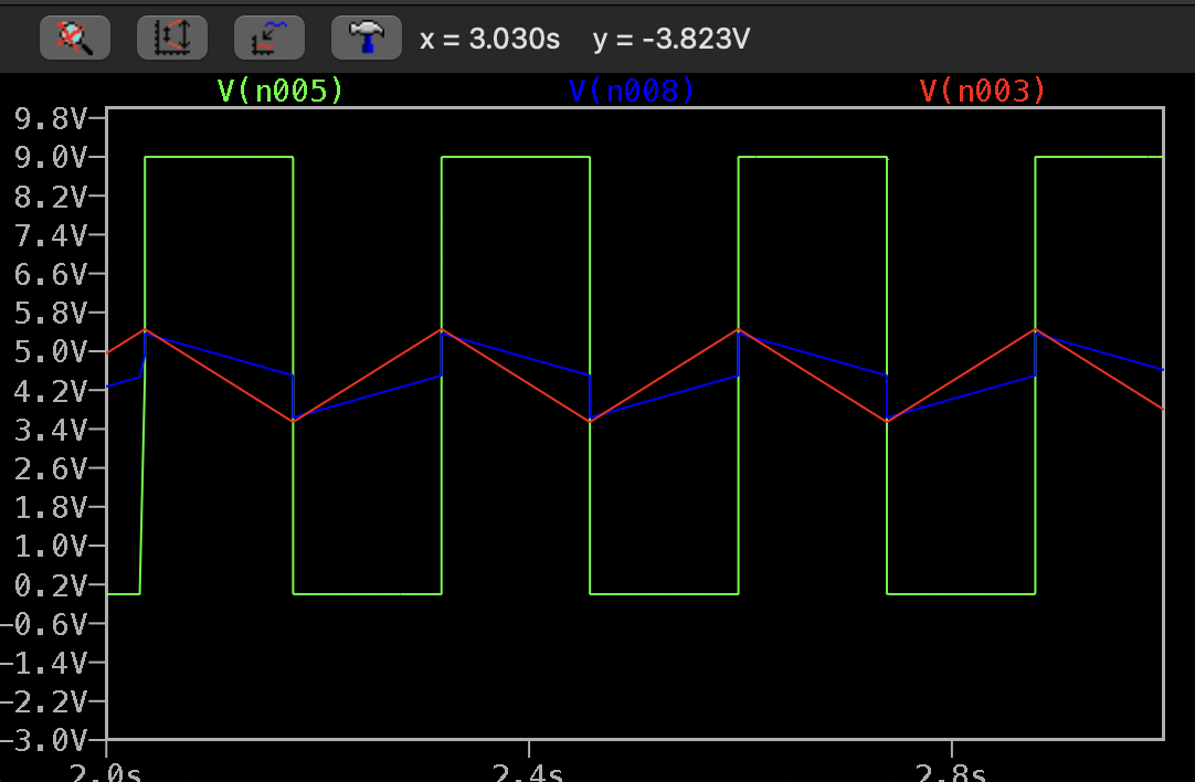
For a mod I replaced the depth knob with a transistor driven by a triangle wave. The wave is generated by a relaxation oscillator composed of a Schmitt trigger and an integrator. I put a potentiometer between them to control the oscillation speed. I fed that triangle voltage signal into the gate of the JFET, which replaces the old Depth knob’s job of controlling the reverb’s mix in the output.
This has the effect of modulating the reverb, producing a shimmering chorus effect which I found a bit cooler.


Well, that’s about it! If you read this far, thank you so much! I had a lot of fun building this pedal and learning about analog design. Below, you can hear how the final pedal sounds.
